
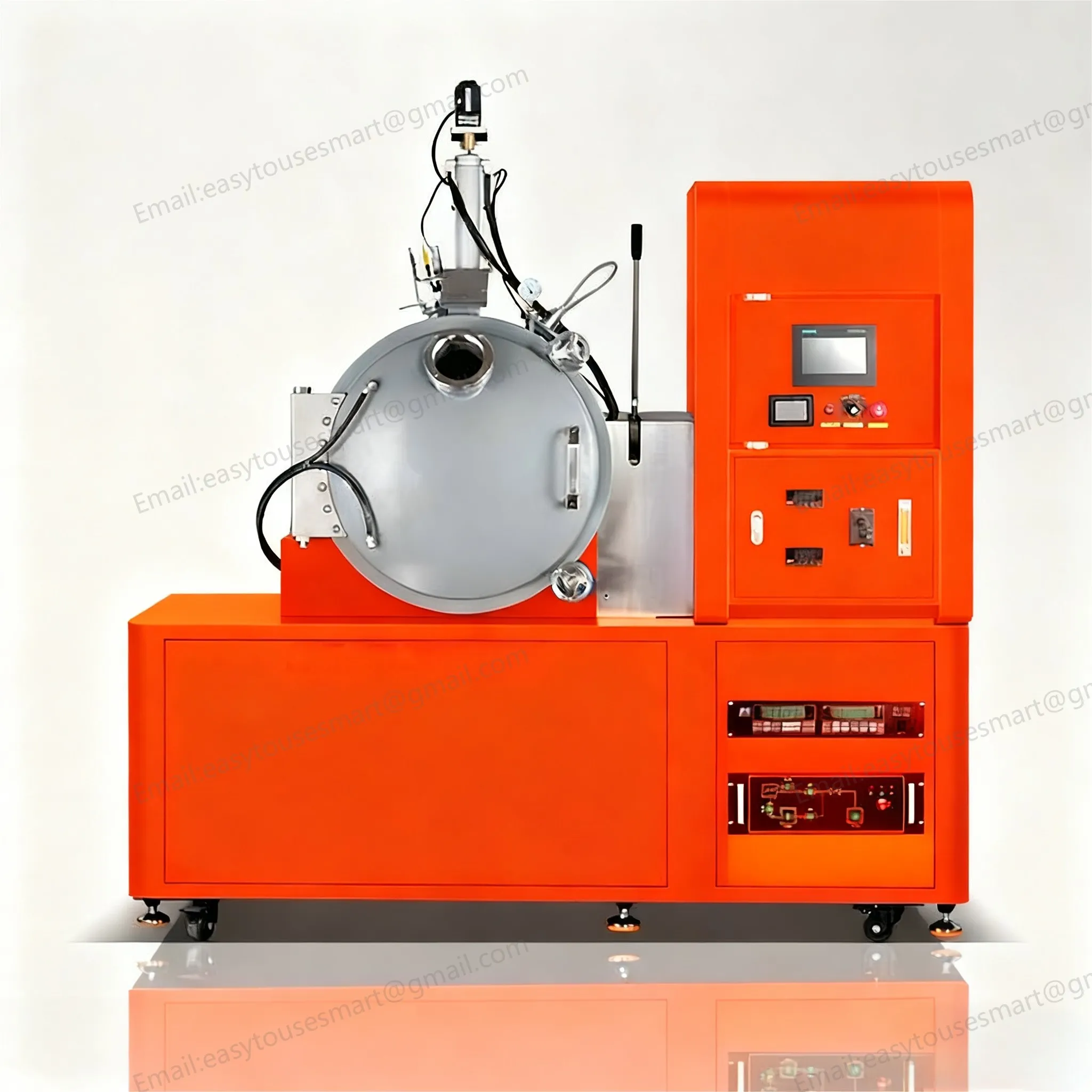
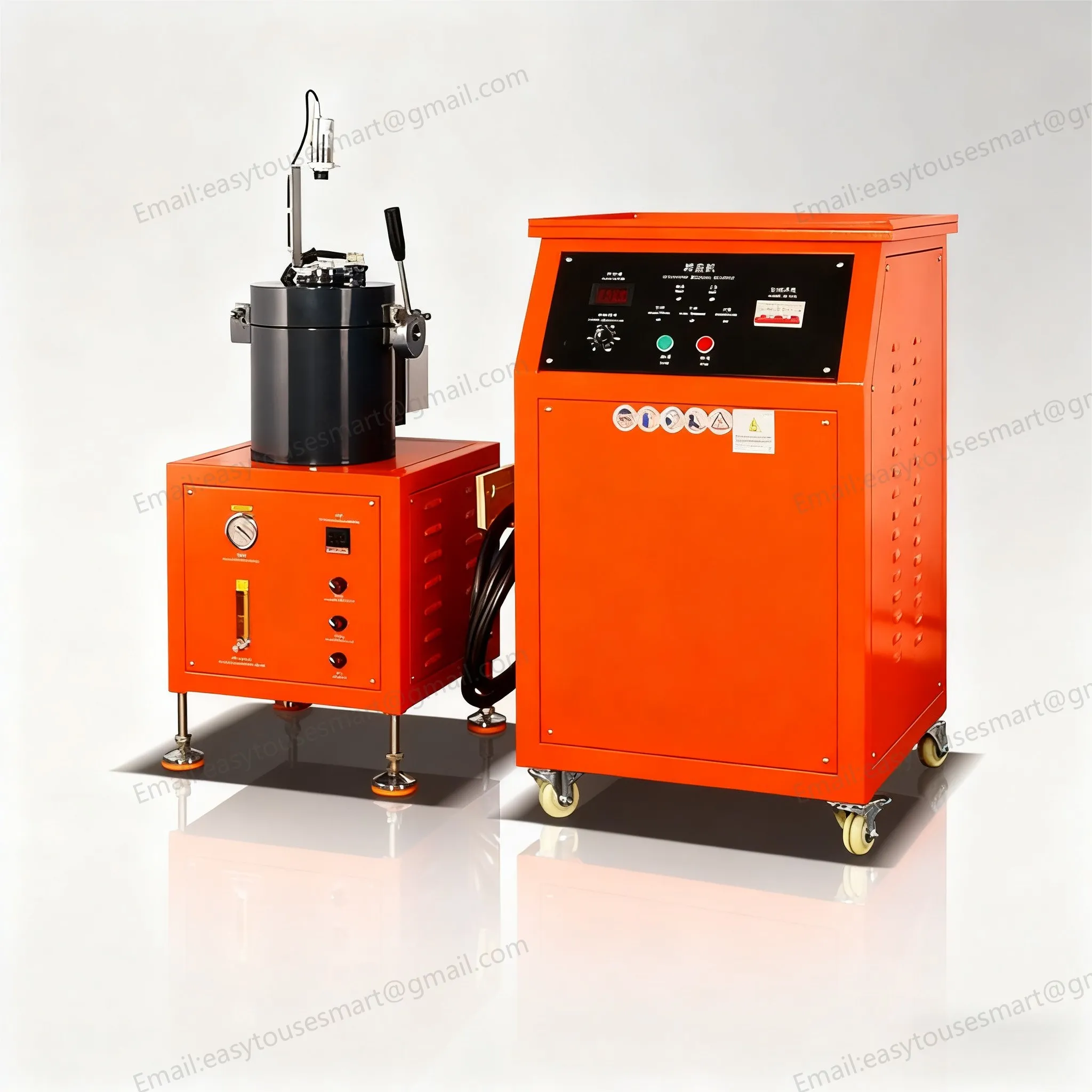
Precision casting with excellent quality
Integrated research and development, manufacturing, sales, and technical services of laboratory scientific instruments and intelligent equipment
National Consultation Hotline 15738867410
Integrated research and development, manufacturing, sales, and technical services of laboratory scientific instruments and intelligent equipment
National Consultation Hotline 15738867410


15738867410
Greenland Binhu International City (District 1), Erqi District, Zhengzhou City, Henan Province
As a core technology in physical vapor deposition (PVD), magnetron sputtering is widely used in semiconductor chip coating, optical film fabrication, and new energy battery electrode manufacturing due to its advantages of low substrate temperature and high-quality thin films. However, insufficient deposition rate has become a key constraint on production efficiency in large-scale manufacturing. The industry's focus lies in optimizing processes to enhance deposition rates while maintaining film quality. This paper details practical solutions for improving deposition rates in magnetron sputtering processes from three dimensions: influencing factors, specific optimization methods, and rate-quality balance, providing technical references for mass production scenarios.
1. Four Core Factors Affecting the Deposition Rate in Magnetron Sputtering
The sedimentation rate is determined by "plasma density, particle energy, target utilization rate, and process compatibility". To optimize it effectively, it is essential to first identify the key influencing factors.
1. Sputtering Power: Directly Determining Particle Yield Efficiency
Sputtering power is positively correlated with deposition rate — higher power delivers greater energy and more atoms to the target, resulting in faster deposition. However, excessive power (e.g., above 10W/cm²) may cause localized overheating, melt the target, increase film internal stress, or even trigger arc discharge. In practice, power density should be maintained between 2-10W/cm², with a target cooling system (e.g., water or air cooling) to prevent damage.
1. Working pressure: Influence on particle transfer efficiency
The working pressure affects the deposition rate indirectly by changing the plasma density and the mean free path of the sputtered particles.
· Low pressure (<0.1Pa): The plasma density is low, resulting in fewer target atom sputtering events and a reduced deposition rate.
· Excessive pressure (>5Pa): frequent collisions between sputtered particles and gas molecules result in significant energy loss, reducing the number of particles reaching the substrate.
The optimal pressure should be adjusted according to the target material type: for metal targets (e.g., Cu, Ag), 0.2-1 Pa is suitable, while reactive sputtering (e.g., TiN, SiO₂ preparation) requires 0.5-2 Pa, which maximizes particle transport efficiency and achieves optimal balance between deposition rate and film density.
1. Magnetic Field Configuration: Determining Plasma Confinement Effect
The magnetic field serves as the core mechanism in magnetron sputtering. By confining electrons near the target material, it increases electron-gas molecule collision probability and enhances plasma density. Inadequate magnetic field design (e.g., insufficient strength or limited coverage) may cause plasma escape and reduce deposition rate. Optimal magnetic field configuration requires: magnetic field strength ≥0.05T (using neodymium-iron-boron magnets), target coverage ≥90%, and non-equilibrium magnetic field design can further expand the plasma region to improve deposition rate.
1. Target properties: Influence on atomic sputtering efficiency
The sputtering yield of the target material (number of atoms sputtered per unit energy) directly determines the deposition rate: high-yield materials (e.g., Cu with 1.2 atoms/ion, Ag with 1.5 atoms/ion) exhibit over 50% higher deposition rates than low-yield materials (e.g., Ti with 0.6 atoms/ion, Al with 0.8 atoms/ion). Additionally, target density (≥95% theoretical density) and purity (≥99.99%) significantly impact sputtering stability—low-density targets are prone to porosity, resulting in uneven particle output and substantial deposition rate fluctuations.
2. Five Specific Methods to Optimize Magnetron Sputtering Process and Improve Deposition Rate
To address these influencing factors, the deposition rate can be systematically enhanced through five key approaches: magnetic field optimization, power supply upgrade, parameter adjustment, target material refinement, and technological innovation.
1. Magnetic field design optimization: Enhancing plasma confinement and improving target material utilization
· High-strength magnets and special configurations: The use of neodymium-iron-boron (NdFeB) high-strength magnets (magnetic field strength 0.1-0.2T) replaces traditional ferrite magnets, increasing plasma density by 30%; an asymmetric/closed-field magnetic structure is designed to confine plasma on the target surface, reducing particle escape and enhancing deposition rate by 25%-40%.
· The introduction of a rotating magnet system: Traditional fixed magnetic fields often result in "uneven etching" of the target material (excessive consumption at the edges and deposition at the center). A rotating magnet (5-10 rpm) can increase the target utilization rate from 50% to over 80%, while ensuring stable sputtering particle output and avoiding fluctuations in deposition rate.
2. Power Technology Improvement: Overcoming Power Limitations and Reducing Energy Loss
· Pulse DC/IFAC power supply: Conventional DC power supplies have low power limits (easily causing arcs), whereas pulse DC power (1-50kHz frequency, 50%-80% duty cycle) achieves 15W/cm² power density without target overheating risks, with 40% higher deposition rates than DC. IFAC power (≈40kHz) is ideal for insulating target sputtering, minimizing arc discharge and ensuring continuous deposition.
· Optimize power supply matching: By employing impedance matching networks (e.g., L-type or π-type matchers), the power output energy is aligned with the target material's load, boosting energy transfer efficiency from 70% to 90% and preventing energy waste-induced deposition rate reduction.
3. Precise control of key process parameters
· Power-pressure synergistic optimization: The optimal combination is determined based on the target material type. For example, Cu targets require a power density of 5-8W/cm² and a pressure of 0.5-0.8Pa, while TiN reactive sputtering demands a power density of 8-10W/cm² and a pressure of 1-1.5Pa. This approach can increase the deposition rate by 30% without compromising film quality.
· Target-substrate spacing and substrate temperature control: An excessively close target-substrate spacing (<50mm) may cause substrate overheating and film roughness, while an overly large spacing (>100mm) increases particle loss and reduces deposition rate. The optimal target-substrate spacing is 50-100mm. The substrate temperature should be maintained between room temperature and-200℃ (≤80℃ for plastic substrates) to avoid high-temperature effects on particle deposition efficiency.
4. Optimization of Target Material Selection and Pretreatment
· High-yield sputtering target materials: Under identical processing conditions, the deposition rates of Cu and Ag targets exceed those of Ti and Al targets by over 50%. When preparing alloy films, select "high-yield element-dominated alloy targets" (e.g., Cu-Ni alloy targets) to balance deposition rates and compositional requirements.
· Pre-treatment and densification of target materials: The purity of the target material is enhanced to 99.999% to minimize impurity interference with the plasma. The density of the target material is increased through hot pressing and sintering (≥98% theoretical density) to prevent uneven sputtering caused by internal porosity. A 10-15 minute pre-sputtering is performed prior to use to remove the surface oxide layer of the target material, ensuring stable initial deposition rate.
5. Optimization of Gas Control in Reactive Sputtering
· Precision control of reactive gas flow: Excessive reactive gases (e.g., N₂, O₂) may form compound layers on the target surface, reducing sputtering rate, while insufficient flow can affect film composition. A gas mass flow meter (e.g., maintaining an N₂/Ar ratio of 1:5-1:8 for TiN sputtering) and feedback control system (e.g., pressure sensors) are required for real-time flow rate adjustment to prevent fluctuations.
· Optimize gas distribution: The multi-channel gas inlet design ensures uniform gas distribution across the target surface, preventing localized overreaction that causes uneven sputtering rates and maintaining consistent deposition rates over large areas.
III. Novel Magnetron Sputtering Technology: Breaking Through the Traditional Rate Bottleneck
Traditional process optimization has a rate limit, while novel technologies further enhance deposition rates through structural innovation or principle improvements.
1. High Power Pulse Magnetron Sputtering (HPPMS)
The system achieves peak power of 1-10kW/cm², with ionization efficiency exceeding 70% (compared to 5%-10% in conventional magnetron sputtering) and deposition rates 2-3 times higher than DC magnetron sputtering. By precisely controlling pulse width (10-100μs) and frequency (10-100Hz), it maintains film density at high rates, making it ideal for semiconductor chip metallization.
1. dual magnetron sputtering system
Two targets (of the same or different materials) are symmetrically arranged and sputtered simultaneously, resulting in a direct doubling of the deposition rate. The alternating sputtering process enables the preparation of multilayer films (e.g., Ti/TiN multilayers), while the dual-target cooling system prevents localized overheating of a single target, making it suitable for mass production.
1. closed-field magnetron sputtering
By employing a special magnetic field configuration (e.g., superimposed magnetic fields of adjacent target materials), the plasma is confined within a closed region, achieving a target material utilization rate exceeding 80% and a deposition rate 30% higher than that of open magnetic fields. Additionally, the plasma exhibits excellent uniformity, making it suitable for high-speed coating on large-area substrates (e.g., photovoltaic glass, automotive panels).
IV. Equilibrium Strategy Between Deposition Rate and Thin Film Quality
To enhance deposition rate while preventing film defects (e.g., pores, stress, excessive roughness), the key balancing strategy is as follows:
1. Determine the process window: Find the "rate-mass" equilibrium point through orthogonal experiments. For instance, in Cu film deposition, when the power density is 8 W/cm² and the gas pressure is 0.6 Pa, the deposition rate reaches 50 nm/min, and the film resistivity is ≤2.0 μΩ·cm, meeting the requirements for conductive films.
2. Substrate bias-assisted: Applying-50 to-200V negative bias attracts high-energy ions to bombard the substrate surface, reducing film porosity and enhancing density. This method prevents increased film stress even when deposition rates are elevated.
3. Post-processing optimization: Low-temperature annealing (200-300°C, 1-2 hours) of high-rate deposited thin films eliminates internal stresses, improves grain alignment, and balances deposition rate with performance. For example, the hardness of TiN films prepared by HPPMS increased from 25 GPa to 30 GPa after annealing, while maintaining the advantage of high deposition rate.
sum up
To enhance deposition rates in magnetron sputtering processes, a multi-dimensional strategy encompassing parameter optimization, equipment upgrades, and technological innovation is essential. The key lies in overcoming traditional rate limitations through improved plasma confinement, enhanced energy utilization efficiency, and optimized target material and gas control. Simultaneously, film quality must be balanced by refining process parameters and post-processing to achieve a "high-rate-high-quality" equilibrium. With the adoption of advanced technologies like high-power pulsed magnetrons and closed-field systems, magnetron sputtering will enable more efficient thin-film production in mass-market applications such as semiconductors, renewable energy, and display panels, thereby meeting the industry's scaling demands.
QR code

Contact information
15738867410
Online Message
Top